TTL-FPGA | | Updated Monday, June 14th 2021, 21:41 |
-- Building an FPGA from 74-series logic ICs. For fun and education.
Technology is becoming more complex every day. Devices get smaller, integration gets higher. Consequently, it is becoming increasingly harder to understand how modern devices work.
In the 80s, you could open your PC and start probing signals on the mainboard to understand which instruction the CPU executed. These days, pretty much everything can be integrated into a single chip and everything is hidden away. One example of such a highly integrated component is the field programmable gate array (FPGA).
FPGAs essentially allow the designer to create large digital designs inside of an IC without having to create actual new silicon. As these designs are created by writing software-like source code, one might easily forget the fact that what is created is, indeed, a digital circuit. The immense overhead to provide this flexibility is easy to underestimate when working with these devices.
To aid students learning about FPGAs better understand the technology, this project aims to provide a platform to look at the inner workings of such a chip by breaking it out of the IC and bringing it onto a PCB where every signal can be traced and measured. Such projects are often done for central processing units (CPUs), but there isn't much when it comes to FPGAs.
Before I delve any deeper into my implementation, I want to highlight that this is only one of many ways to construct such an "FPGA." Also, this project does not accurately represent the circuits inside a commercial FPGA. Many things, especially the routing, had to be grossly simplified in order to be feasible. The basic concepts, however, should still hold true.
Resources
WARNING: Before you go ahead and build one of these yourself, be aware that the current revision has a (minor) errata. See below for more info.
Here's a quick list of links to all important information regarding the TTL-FPGA:
- Git repository [1] (Software on branch "sw")
- PCB schematic [2] (layout optimizations, use this to understand the specific implementation)
- Clean schematic [3] (use this to understand the concept, config bit numbers are different!)
Architecture
Overview. The TTL-FPGA consists out of individual logic cells, each able to perform a very limited function. By combining many of these elements, a more complex function can be realized. For all further explanations, let's assume we arrange the logic cells in a 4 by 4 grid. Each cell has inputs and outputs on all four sides. The resulting overall architecture is shown in Figure 2.
The inner construction of a logic cell can be seen in the middle part of the figure. It can be roughly split into four sections.
Input selection. A multiplexer allows to select which of the 12 inputs (4 top, 4 left, 4 right/bottom/feedback) is used for each of the 4 lookup table inputs.
Lookup table. The lookup table contains the actual logic function. For each combination of the inputs to the LUT, a single output is provided. A LUT in this architecture can have up to 4 inputs. Alternatively, the logic can be split into two 3-input LUTs. In this case, the cell can calculate and drive 2 independent results to subsequent parts.
Sync. Each cell stores the result of the LUT result upon the rising edge on the clock line.
Output driver. A set of combined multiplexers and tri-state buffers allows to drive the result of either LUT result (LUT3 A or B, or LUT4) to any of the four output lines on the right and bottom. This result is also fed back to the input multiplexer so that a logic function can depend on its own output (delayed by a clock cycle).
Routing. The routing options are shown in the lower part of the graphics. Each line can only be connected to its corresponding counterpart on another side. Lane 0 on the left can only connect to lane 0 on top, bottom, or right. If a lane switch is required, the signal must be routed through a transparently configured LUT whose output is driven to the desired lane. The right and bottom buses are hardwired together. This net can be connected to either top, left, or both on a lane-by-lane basis.
LEDs
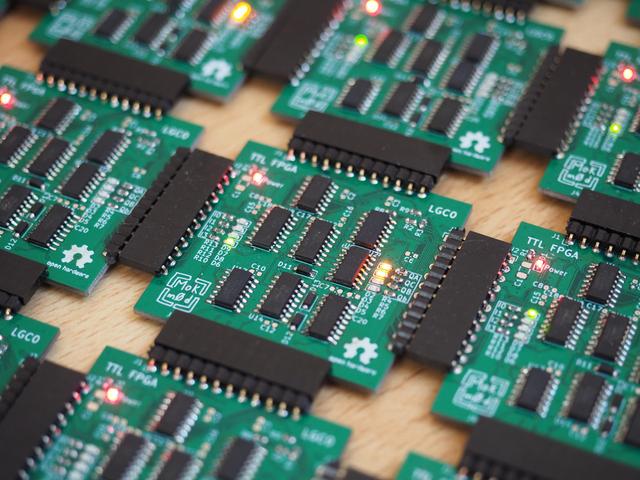
Each logic cell board has a total of 9 LEDs to illustrate the current state of the logic cell.
The power LED (red) is lit as soon as the board is powered.
The green LEDs on the left side of the board indicate the state of the selected LUT inputs.
The orange LEDs on the right indicate the state of each LUT output. Even though their meaning might be irrelevant, all LEDs will light up regardless of the selected mode (split LUT-3, or single LUT-4).
Programming
One thing omitted in Figure 2 is the SPI-programming chain. Each logic cell features 48 bits of configuration memory used to configure the multiplexers, drivers, and LUT of that cell. This configuration memory is organized as a long serial-to-parallel shift register. In a completed setup, the cells are wired so that all logic cells form one long configuration shift register. This means that, to configure the FPGA, the bit stream needs to be clocked into the configuration port of the first cell, starting with the configuration data for the last cell, and finishing with the first.
In this prototype, an AtMega based microcontroller is used to provide a USB-to-SPI bridge.
Software
Hardware is only half the deal for an FPGA though, or most likely even less. To make use of the hardware, we need some piece of software to turn our idea of what the design should do into a bit-pattern that configures the individual logic elements appropriately.
For FPGAs, these tools, or the corresponding steps, are usually called
- synthesis: Turning a hardware description language definition into a netlist.
- translate / map: Map the elements from the netlist onto the actual hardware present on the FPGA.
- place and route: Select the location for these elements and generate the routing between them.
As such, a simplified software to directly configure each logic cell is provided. This essentially leaves the designer with the job to do the synthesis, mapping, and place and route themselves. This software will then take these configuration parameters and generate a bit stream, which can then be clocked into the FPGA's programming input. For the TTL-FPGA, this software is called Kousaten [1].
Note: Right now, the software does not read the FPGA cell configuration from a file. The configuration is hardcoded in the C source code along the actual application. So recompiling and executing is required for each bit stream.
Each logic cell of the TTL-FPGA has the following configuration options:
- lut_in_sel[3..0]: Input selection for the LUTs. Can be any of LUT_NET_*. Some configuration options are invalid, the tool will report an error in this case. Refer to the schematic (LUT Input Muxing) for more information on possible combinations.
- sync: Switch the cell into synchronous mode. Setting this bit will enable the flip flops on the A, B, and C outputs. Output b will always stay asynchronous.
- drive_sel[3..0]: Output configuration for the specific net. Can be 'Z' to not drive the line (e.g. when using the net for routing), or A (LUT-3 0), B (LUT-3 1), C (LUT-4), or b (LUT-3 1 always asynchronous). Driving a net will drive the value to the right and down. Some configuration options are invalid, the tool will report an error in this case. Refer to the schematic (LUT Output Muxing) for more information on possible combinations. Note: When configuring the cell for split 3-input mode, the 'C' output can still be selected. In this case, it will hold the logical OR of the two LUT results.
- route_en: Enable routing from top or left to bottom / right. Bottom and right are always connected. Setting the ROUTE_* bits on this variable will connect the selected line to the right / bottom net with the same number. Routing to a different number is not possible with routing resources alone, a LUT-3 or LUT-4 has to be used for this purpose.
- LUT3[1..0], LUT4: LUT contents. LSbit represents input 0. Only fill either the LUT-3 or LUT-4 contents. Setting both will raise an error.
An Example: 16-bit counter
To make the whole process a little clearer, let me explain it for creating a basic 16-bit counter.Figure 3 shows the block level schematic of a possible implementation of a basic 16-bit counter. Such a counter can be efficiently implemented using the split cell mode. Each cell will then contain a) the counter register, and b) the logic to determine when to increment the next position.
The counter register portion needs to be configured so that its logic value toggles when the all previous counter bits are in a '1' state. In any other case, it should keep its value. As the FPGA architecture does not feature clock enables, this has to be accomplished by feeding back the register value into the LUT. The first cell will not have any previous state, therefore, this input bit functions like an enable signal.
The second part of the logic cell needs to generate the signal to tell the next cell that all previous cells are in a '1' state. Let's call that signal the AND-result. This can be accomplished by performing a logic AND on the value of the local counter register and the AND-result fed from the previous cell.
For these functions, only two inputs are needed per LUT, which easily fits even into the split 3-input LUTs. As the first result is registered, the cell needs to be switched into synchronous mode. The 'b' output can still be used to access the second LUT's output asynchronously.
Depending on the layout of the counter (in this case left-to-right, top-to-bottom), the AND-result needs to be fed back at the end of each row to the beginning of the next. At the same time, the first cell needs to pick its AND-result from the top instead of the left.
This functionality can be implemented using the following configuration for each cell. first is set to 1 for the first logic cell in a row, last is set to 1 for each last cell in a row.
This then needs to be called for each cell in the 4x4 FPGA to generate the 16-bit counter.
Finally, to generate the bit stream, Kousaten needs to be recompiled and executed:
make && kousaten -f ../fdef/4x4.fdef -o counter.bin
The bit stream can then be copied to the device using:
stty -F /dev/ttyACMx raw && cat counter.bin > /dev/ttyACMx
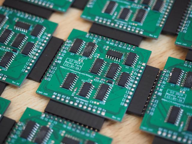
Take a look at the gallery below for videos of the running example.
Implementation of the TTL-FPGA
Next, I want to quickly go over how this functionality has ben realized on the schematic level. To understand this, best open the clean schematic [3]. This schematic is not directly equivalent to the actual circuitry on the board as it does not include optimizations made during the layouting stage, which does make it more readable, however. These changes move configuration bits, but will not change the overall concept of the design.
Programming chain. Let's start with the top level schematic on the first page. This page shows how the TTL-FPGA's individual logic blocks are supposed to be used and connected. This page is mainly useful to understand the routing of the programming SPI chain. Refer to chapter Programming for more information on this.

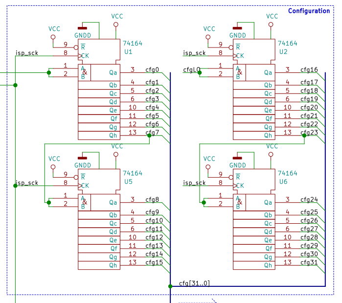
Bit stream. While we're on the topic of the configuration bit stream, let's look at how it is stored. The serial-in parallel-out shift registers (74164) U1, U2, U5, and U6 on page 2 are used to store all configuration bits besides the actual LUT content. After being shifted in, the configuration data will be statically available on a wire. As there is no latch pin on the registers, the configurations will inevitably be invalid while loading the bit stream, which causes all the flashing during programming seen in the gallery below.
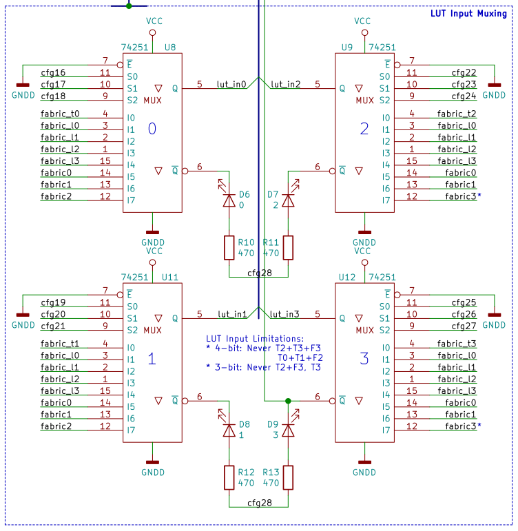
Input muxing. Input muxing is pretty straight forward. There's a total of 12 inputs (4 top, 4 left, 4 feedback/right/bottom) to map to 4 inputs on the LUT. As there is no reason to feed an input into the LUT more than once, and as the order doesn't matter (it can always be swapped inside the LUT), a 9-input multiplexer is enough to cover all combinations. 9, however, is quite an unfortunate number when it comes to these ICs as they're usually only available in powers of two. After weighing the increased complexity of using compound 9-bit multiplexers, I decided to disallow some specific input combinations instead and make use of the 74251 8-input multiplexers. These impossible combinations are denoted on the schematic.
Lookup table + register. The lookup table logic (LUTD) can be found on page 3 of the schematic. In theory, a lookup table is nothing but a RAM block, in our case one with 4 address lines. The address represents the lookup table input, the output of the RAM cell represents the output. Only problem is, there's practically no market for RAMs this small, and consequently, they're not available. At the same time, even if we had a 16-bit RAM, how would we get our LUT data into it? So back to the drawing board it is. Turns out there's a better approach to this in general: We build our own serial-in, addressable-out memory logic. 16-bits of serial-in, parallel out storage is easy. We just use two 74164s that we've already used for our configuration storage. In the next stage, we could use a 16-bit multiplexer (which has four select lines) to address each of the bits and therefore create our addressable RAM block. However, I wanted to be able to split the single 4-input LUT into two 3-input LUTs to double the logic density for simpler logic functions. So let's first work with two 3-input LUTs. Again, nice, we can reuse the 74251 demultiplexers we already used in the input selector, bringing our BOM down. These outputs (async_a, async_b) can now be registered using a flip flop (74174), or used directly for asynchronous functions. The selection between the asynchronous and synchronous path is accomplished using a 74157.
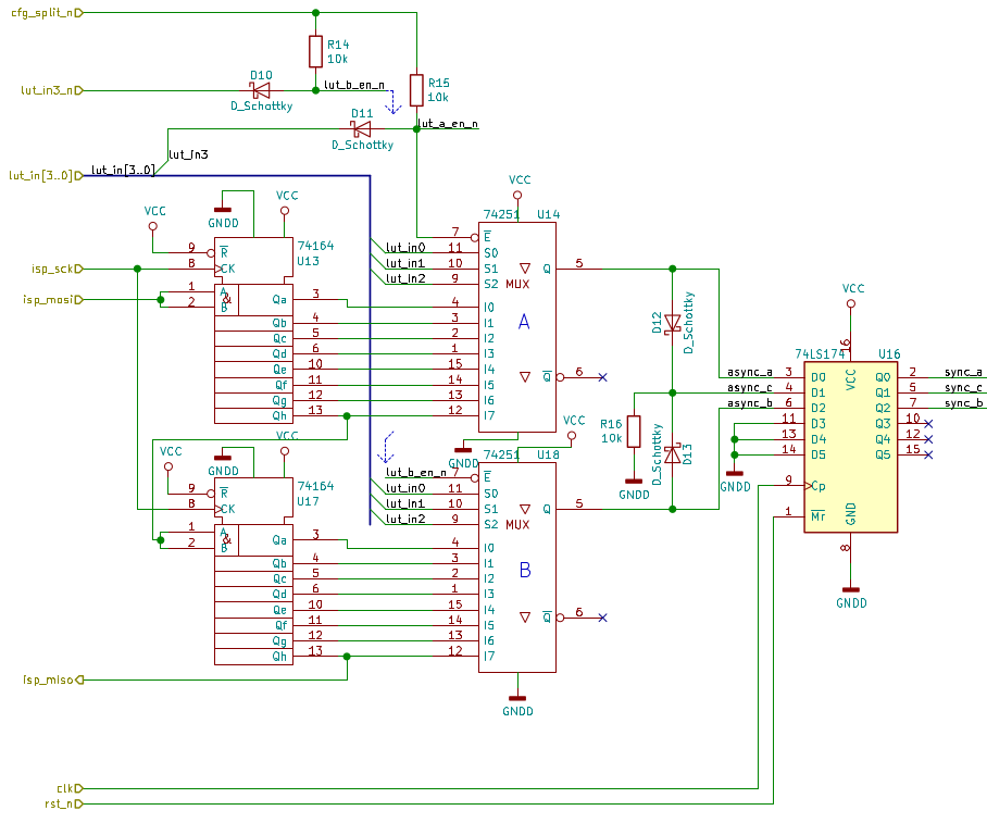
We now have the 3-input LUT functionality working, so back to making the larger variant work. We could just use a 16-bit mux to generate the output for that, but these chips are physically large and expensive, and with the "preconditioning" done by the two 74251 8-input muxes, there just had to be a simpler way, and there is. For the lower three bits, the 3-input and 4-input modes do exactly the same. The 4-input mode just needs to aditionally select between the output of either 3-input mux depending on the value of the fourth input line. All diodes and resistors on this page of the schematic realize this functionality. Let's go through it.
When the lut_in[3] input is low, we need to select the top mux's output. If we can guarantee that the other LUT output is low (or high impedance), we can just append a logic OR function and we get our value. Similarly, when lut_in[3] is high, we need to select the bottom mux's output, so the top mux needs to be disabled. Luckily, the 74251 muxes have an enable pin, so all we need to do is to create a logical OR on the output, and use the fourth input (and it's inversion) to drive the enable signal on the 8-input LUTs.
That's what's done here. D12, D13, and R16 form a diode-based or gate. The enable signals of the muxes are wired through to lut_in[3] and lut_in_n[3] (which we luckily get for free from the input muxes). The additional diode-logic consisting out of R14 + D10 and R15 + D11 each create a NOR gate, ensuring that both flip flops are active when the cell is in split mode (as both outputs need to be always enabled in this case). This combined output is then also fed through a flip flop to provide a registered version of the signal.
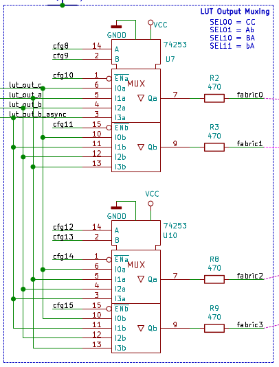
Output muxing. The LUT + register (LUTD) core provides 4 output signals (LUT-3 A, LUT-3 B, LUT-4 (C), and asynchronous LUT-3 b). The output muxing circuitry provides the means to route each of these signals to any of the four fabric lines (connected to right / bottom / feedback), or none. The 74253 is almost perfect for the job. It consists out two 4-input muxes (which is the amount of outputs from the LUTD-core), which can alternatively individually be set to tristated. This is important as signals are supposed to be able to be routed through a cell without being affected by the logic implemented on that cell. The only downside to the 74253 is that the two muxes on one chip share the same select lines. Therefore, only predefined combinations can be routed to two adjacent nets. However, this problem only occurs when using split mode, and also then only when using the always asynchronous b output. To make things even less problematic, the content of LUT-3 A and B can be swapped along with the input map to appear on a more convenient output line. WARNING: There is an errata regarding the output muxing block. Read "Errata" below for more info.
Routing. The last part to discuss is the routing of signals through the cell. By default, a logic cell's result is routed to the right and bottom ports only. If a line is left undriven, it will remain in a floating state. The aim was to be able use any line that is not used by the cell as routing in either direction. A good choice for a bidirectional buffer (assuming no long signal paths) is an analog switch such as the 4066 used in this design. This chip provides 4 lines, which can be connected just like a relay by applying a control voltage. Otherwise, they're high-impedance on both ends. The routing doesn't have to be changed on the fly by the logic, so we just hook it up to some configuration bits.
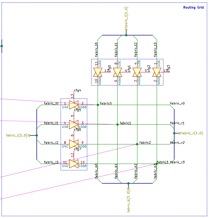
These analog switches are only required on the top and left end of the cell, and not on the right or bottom as these sides are "shielded" by the cell connecting to that end. Remember, in the final array, each bottom will have a corresponding top, which then has the switch.
Errata
Revision 02
Output LUT
Problem: Combination BA is not possible on the output drivers, will be BB instead.
Solution: Cut U7 pin 12 (B), connect to 13 (A) for the upper LUT. Leave the lower LUT as is. This is not a 100 % solution, but acceptable for the first prototype. For more information, see Issue #12 [6].
Input Silkscreen
Problem: The silkscreen marking the input LEDs is reversed. I0 is I3, I1 is I2 and vice versa.
Evaluation and Summary
This for sure was a very interesting experiment. The largest challenge when creating the TTL-FPGA was the trade-off between flexibility and circuit complexity. Many boards have to be built, so it is a target to keep cost and size down; Yet, at the same time, reducing configuration and routing options will greatly impact the designs that can be realized using the architecture.
The TTL-FPGA tends to not be flexible enough for more complex designs, especially regarding its routing options for far distances. Routing a signal often greatly reduces the usability of the cell the signal is routed through.
With that being said, the TTL-FPGA still achieves the main goal of the project: To illustrate how an FPGA functions internally. All signals can be probed using an oscilloscope or logic analyzer while running basic examples like counters, shift registers and basic boolean functions.
All information necessary to build your own can be found in the Git repository of the project [1]. If you have any questions or need help regarding this project, please don't hesitate to contact me.
Gallery
Embedded content has been disabled to protect your privacy.
or click here to allow them permanently,
or click here to watch the video on YouTube:
https://www.youtube.com/watch?v=NiBkQ1kTp7o
Please note that, by enabling this video, data is transferred
to YouTube LLC, and is subject to their privacy policy.Embedded content has been disabled to protect your privacy.
or click here to allow them permanently,
or click here to watch the video on YouTube:
https://www.youtube.com/watch?v=ZvwuIMMED4o
Please note that, by enabling this video, data is transferred
to YouTube LLC, and is subject to their privacy policy.Embedded content has been disabled to protect your privacy.
or click here to allow them permanently,
or click here to watch the video on YouTube:
https://www.youtube.com/watch?v=nPS1z4wORI4
Please note that, by enabling this video, data is transferred
to YouTube LLC, and is subject to their privacy policy.
Sources:
[1]: https://git.notsyncing.net/electronics/ttl-fpga
[2]: https://git.notsyncing.net/attachments/dfe2fdf4-558a-4b0b-9856-c2b1b4196deb
[3]: https://git.notsyncing.net/attachments/e0a7a169-918e-4f0f-b577-0f5b18b6ceed
[4]: https://github.com/YosysHQ/yosys
[5]: https://github.com/YosysHQ/nextpnr
[6]: https://git.notsyncing.net/electronics/ttl-fpga/issues/12
