Leddie | | Sunday, July 7th 2024, 19:17 |
-- A simple 6-sided die with LEDs.
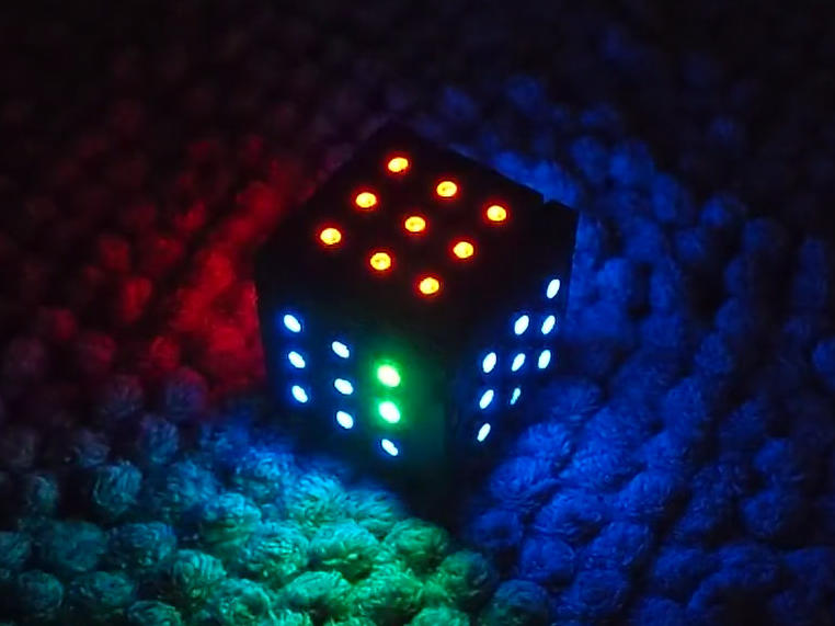
Leddie is a 6-sided die with nine RGB LEDs on each side. This first prototype is powered by an Atmega8 and an accelerometer, and can off the wall for about two hours thanks to the built-in 400 mA li-polymer battery.
A little bit of history
I technically started this project about 3 years ago, but didn't work on it for long spans of time. I started out with an Atmega8 knowing it would be underpowered for what I want to do, yet went ahead with it because I need I would a) be able to get a demo running very quickly on it, and b) because I knew I could achieve my ultra-low power standby modes (Leddie does not have a power switch, the CPU is always connected to the cell.) Mid-project I decided that, ultimately, I'd want a WiFi-connected chip in there so that I can sync multiple dies across the Internet to aid, for example, in remote DnD campaigns. That, in combination with the usual curse of getting interested in new projects before finishing the old ones, made me put the project on hold. When I rediscovered the project many months later, I looked at the state I had left it in -- all board layouts completed, pretty much unreviewed, and with the Atmega8 -- and decided to just go for it and order everything in the current state. The idea was that there would probably be some things that need changing, so I could use this Rev 1 to learn and iron out the basics, and then fix all of those along with the CPU upgrade in a Rev 2.
Mechanical Construction
One goal from the start was that the cube should not consist of any parts other than the electronic components and the PCB. No 3D-printed housing, no other mechanical parts.
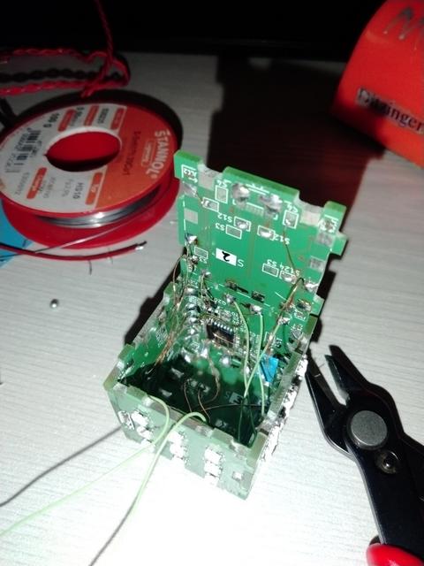
Therefore, the construction was inspired by how many laser-cut wood panels are assembled. Pieces are aligned using little notches, and are then directly soldered to each other. The additional advantage of soldering them is that the mechanical connections can double as electrical ones.


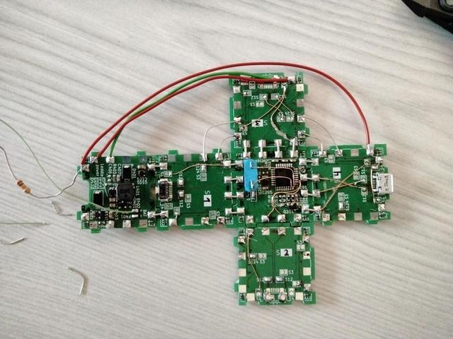
In terms of PCBs, there's a bottom PCB handling power, a top PCB handling the CPU + accelerometer (all things digital), and side PCBs with the charge/data port and switch. Each PCB has the necessary components for these functionalities on the inside while the outside is always covered in 9 RGB LEDs. The boards are described in more details in the next section.
Electronics
Power
The power board has three main responsibilities:
- Provide 3V power for the CPU
- Provide 5V power for the LEDs
- Handle charging of the 400 mAh 3.7V LiPo battery
The 3V supply is used to power the CPU and accelerometer. It must always be active as the system must be able to wake up from the "off" state using the same button that is used for normal user interactions. This is implemented using a simple low-dropout regulator (LDO) from the battery voltage to the CPU supply rail. This means that the CPU voltage will vary from 3.3V (regulated) down to 3.0 V when the battery runs low. The power supply to the accelerometer is technically a separate power rail, but to save components, its power is switched directly through an I/O pin of the microcontroller, basically abusing it's output FETs and power MOSFETs. This is acceptable because the supply current of the accelerometer is lower than the Atmega's drive capability.
The 5V supply is required to drive the WS2812B LEDs. As this voltage is higher than the battery voltage, and quite some current can be required for, for example, bright pulses of all LEDs, this one is implemented as a switch-mode power supply (SMPS). Additionally, a MOSFET is added before the regulator to switch completely switch it off when the device is in standby.
Battery charging is implemented using an integrated linear charge controller. Nothing fancy here.
Digital (CPU + accelerometer)
The digital board implements all logic functionality of the die:
- Processor
- Accelerometer
The microcontroller is an Atmega8 by Microchip (formerly Atmel), which is based on the 8-bit AVR-architecture running at 16 MHz. This microcontroller implements runs the entire program logic controlling the LEDs, power systems, and USB communications.
USB functionality is implemented using V-USB [1], which implements USB 1.0 by bit-banging the I/O ports of the AVR. On the hardware side, it only requires a the USB D+ and D- lines to be connected to the chip through an 68 Ohm resistor each and a 1.5k pullup on D-.
To control the WS2812B LEDs, their voltage is shifted from the 3.3V that the microcontroller operates on to the 5V of the LEDs. Note: In the current revision, this is implemented as a simple NPN bipolar transistor with a pullup. This circuit, however, is not fast enough to properly drive the waveform the LEDs need. As a workaround, the level shifter has been removed entirely which appears to work as the LED voltage has been reduced to around 4.5V.
The accelerometer on the board is an MMA8653FCR1, which provides acceleration data on 3 axes. Additionally, it implements drop and tap detection, and is wired to interrupt inputs on the AVR, which allows, for example, to wake the die from deep sleep simply by picking it up.
Sides
TODO
Power Consumption
TODO: Idle, all-on, sleep power consumption.
Errata
The long long list of errata... As I just grabbed the design files in whatever state they were in when I rediscovered the project many months after stopping, many errors made it through the cracks. I'll attempt to list them here, but no guarantee that I've caught all.
- Atmega8 missing crystal: For USB, we need a 16 MHz crystal. Workaround: Bodge it on the PCB.
- Atmega8 supply voltage: The Atmega 8 is not specified to function properly when operated at 3.0V@16 MHz. Workaround: It appears to work :shrug:
- Pinout side PCB mirrored: On all sides, the top/bottom connectors are mirror flipped (GND should be PWR, 2 should be 3 etc.). Workaround: Cut and strap.
- WS2812B level shifter too slow: The NPN+Pullup level shifter is too slow. Workaround: Directly connect the Atmega to the WS2812B, seems to work fine as I run them at 4.5V instead of 5.0V...
Videos
| Embedded content has been disabled to protect your privacy. or click here to allow them permanently, or click here to watch the video on YouTube: https://www.youtube.com/watch?v=FE6J7YIEzy0 Please note that, by enabling this video, data is transferred to YouTube LLC, and is subject to their privacy policy. |
| Embedded content has been disabled to protect your privacy. or click here to allow them permanently, or click here to watch the video on YouTube: https://www.youtube.com/watch?v=x5G-noaqAK4 Please note that, by enabling this video, data is transferred to YouTube LLC, and is subject to their privacy policy. |
Sources:
[1]: https://www.obdev.at/products/vusb/index.html

